
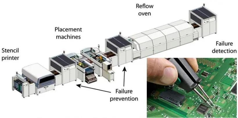
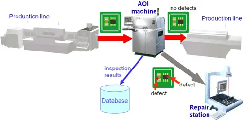
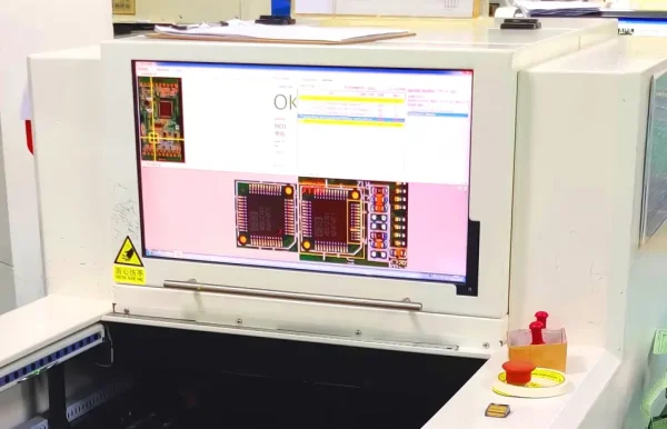
Step 3: Automated Optical Inspection (AOI) Prior to Reflow
It is critical to examine after completing component placement since whether components are connected correctly or not can affect the PCB’s overall function. Using an AOI machine to check for component presence, type/value, and polarity is the ideal method to do this.
Step 4: Reflow Soldering
Reflow soldering is a technique in which a solder paste (a sticky mixture of powdered solder and flux) is used to temporarily link one or more electrical components to their contact pads, and then the entire assembly is heated to melt the solder and permanently connect the junction. Passing the assembly via a reflow oven or under an infrared lamp, or soldering individual joints with a hot air pencil, are all options for heating.The most typical technique of attaching surface mount components to a circuit board is reflow soldering, however through-hole components can also be attached to a circuit board by filling the holes with solder paste and inserting the component leads through the paste. Reflow is rarely utilized on pure through-hole boards since wave soldering is easier and less expensive. Through-hole reflow eliminates the wave soldering step from the assembly process when utilized on boards with a mix of SMT and THT components, potentially lowering assembly costs.

Step 5: Automated Optical Inspection (AOI) After Reflow
The final step in the surface mount assembly process is to double-check for errors by using an AOI machine to inspect solder junction quality. The movement during the reflow process might sometimes result in poor connection quality or no connection at all. In other words, because misplaced components can sometimes join areas of the circuit that should not connect, shorts are a common side effect of this movement. As a result, inspection after reflow soldering is critical, and checking for these faults and misalignments can be accomplished using a variety of inspection methods.The following are some of the most prevalent examination methods:
1.Manual Inspections
2.Optical Inspection (Automatic) (AOI)
3.X-ray examination by computer (AXI)
Step 6: X-Ray Inspection
Any boards with BGA, QFN, or other lead-free package types are sent for X-Ray Inspection following a reflow cycle; this service is by default included in all Yingstar quotations that include such parts.
Advanced image processing software, like Automated Optical Inspection, can analyze the image of the solder joints themselves created when X-rays penetrate the silicon of an IC package and reflect from the metal contacts under it . Darker images are produced as a result of the captured area’s higher density features, enabling quantitative analysis to assess the solder joints’ quality and compare it to industry standards.
The analysis of an X-Ray image can help to identify the underlying cause of a given defect, such as inadequate solder paste, crooked part placement, or an incorrect reflow profile, in addition to detecting problems with PCB assembly.
Below are procedures implemented after SMT Assembly finished:
Wave Soldering
A conveyor is used to move boards through a “wave” of molten solder as part of the wave soldering PCB assembly technique. Through hole parts will benefit from this technology, which will be much faster and less expensive than manual soldering. For your boards, our engineer will create a wave soldering fixture that will hold them and protect the SMD components while only exposing the pins of the through-hole components to the molten solder. It’s the best option for soldering through hole components because it’s low cost, high speed, and produces fewer errors.
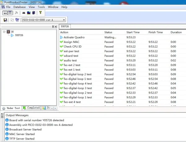
Final Inspection and Functional Test
After SMT assembly and through hole parts assembly completed, the Quality Assurance team will do a final inspection to ensure the PCB’s functionality. A “functional test” is the term for this type of inspection. The customer normally provides the test software and tools, but the we can also create functional testing fixtures to meet the customer’s needs. Then our testing teams will burn the software to the main chip and start the testing. The test puts the PCB through its paces by imitating the PCB’s usual operating conditions. In this test, testers examine the electrical characteristics of the PCB as power and simulated signals are sent across it.
Cleaning and Drying
Because oil and grime are present throughout the manufacturing process, the PCB is cleaned and dried before being shipped. Soldering paste, for example, leaves some flux behind, and human handling can transfer oils and grime from fingers and clothing to the board’s surface.
Conformal Coating
After PCB Assembly finished, some customers will need their boards to be conformal coated. Conformal coating is a thin polymeric film that adheres to the contours of a Printed Circuit Board to protect the components on the board. It is typically sprayed on electronic circuitry at a thickness of 25-250 m (micrometers) to protect it against moisture, dust, chemicals, and temperature extremes. If the electronics are not coated (protected), they may be damaged or fail to work. Conformal coatings or potting compounds provide protection for devices that must tolerate hostile conditions or impact.Most circuit board assembly shops employ a transparent conformal coating instead of potting because it is lighter and easier to check.
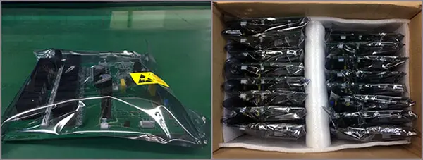
Packaging and Shipping
All assembled boards are packaged (anti-static packaging is available upon request) and dispatched via various courier services like as DHL, FedEx, UPS, EMS, and others. Unused components are returned to the buyer according to their instructions. Customers are also notified through email when their products are shipped. The following are some examples: