PCB Fabrication Capabilities
Home » PCB Fabrication Capabilities
PCB Manufacture
Our PCB facility has over 500 competent employees and twelve cutting-edge production lines. We provide Prototype, low-volume and Production PCB fabrication services for rigid, flexible, rigid-flexible, and aluminum boards. Each job is delivered on time and with a guarantee of quality.
Rigid PCB Manufacture Capabilities
ITEM | TECHNICAL PARAMETER | ||||||||||||
LAYERS | 1-60 | ||||||||||||
Max.Board Size | 680mm×1000mm | ||||||||||||
Board Thickness | 0.25-6.0mm 10mil-152.4mil | ||||||||||||
Min. Line Width | 0.075mm 3mil | ||||||||||||
Min Space | 0.075mm 3mil | ||||||||||||
Min Hole Size(Mechanical) | 0.2mm 8mil | ||||||||||||
Min Hole Size (Laser) | 0.10mm 4mil | ||||||||||||
PTH Wall Thickness | >0.025mm 1mil | ||||||||||||
PTH Hole Dia Tolerance | ±0.076mm 3mil | ||||||||||||
Non PTH Hole Dia Tolerance | ±0.05mm 2mil | ||||||||||||
Hole Position Deviation | ±0.05mm 2mil | ||||||||||||
Outline Tolerance | ±0.13mm 3mil | ||||||||||||
V-cut | 30°/45°/60° | ||||||||||||
Impedance Control | +/- 7% | ||||||||||||
Fire Resistance | 94V0 | ||||||||||||
Max copper weight(inner) | 6 oz | ||||||||||||
Peel-off Strength | 1.4N/mm | ||||||||||||
Soldermask Abrasion | >7H | ||||||||||||
Solderability Test | 260℃20 second | ||||||||||||
Flammability | 94v0 | ||||||||||||
E-test Voltage | 50-300v | ||||||||||||
Bow/Twist | ≤0.75% | ||||||||||||
Surface Finishing | HAL、Entek、Flash gold、Gold finger、OSP Immersion gold、Immersion Tin、Immersion Silver、Lead free HAL |
||||||||||||
Base Laminate Type | FR4,Tg 130℃/Tg170℃,Aluminum base,Rogers, (taconic、Arlon、Nelco、Isola…),Halogen free | ||||||||||||
PCB fabrication capabilities refer to the ability of a PCB manufacturer to produce various types of printed circuit boards. Nowadays, the most popular types PCB is rigid PCB, and it is used in almost all electronic product. And the materials for rigid pcb manufacture usually are FR4 tg130-150℃/ tg170-180℃, Aluminum & Copper base,Rogers, (taconic、Arlon、Nelco、Isola…),Halogen free,etc. Among those materials, FR4 tg130-150℃is most widely used for rigid PCB manufacture, as it can meet most needs of common electronic apparatuses, such as consumer electronics, general instruments, common industrial electronics and all other electronic products with low running temperature. And the second most widely used material for rigid PCB manufacture is Fr4 tg170-180℃, it is widely used in computers, communication equipment, precision instruments and meters, military products and high-precision diagnosis and treatment equipment. Rigid PCB can be single layer and multi-layer, Yingstar has strong rigid PCB manufacture capabilities, we can make multi-layer rigid PCBs up to 60 layers.
The second most popular types of PCBs is the flexible PCB. As the name suggests, these PCBs are flexible, allowing for more versatility in their use. flexible PCB manufacture is a complex process that involves the use of specialized materials and equipment.
The process of flexible PCB manufacture starts with the design of the board using CAD software. The design is then transferred to a specialized material, which is typically made of a flexible polymer. The next step involves the use of a laser to drill holes for the electronic components and then applying a layer of conductive material onto the board. Once the conductive layer is applied, the board is laminated to add strength and durability. Finally, the board is cut to the desired shape and size.
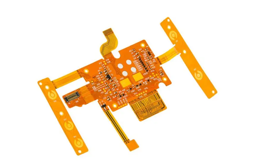
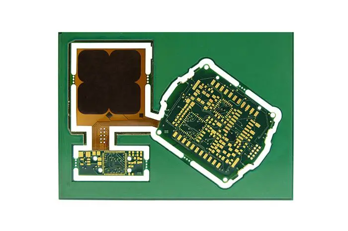
Another popular type of PCB is the rigid-flex PCB. This type of board combines the advantages of both rigid and flexible PCBs, allowing for greater design flexibility. Rigid-Flex PCB Manufacturer is a more complex process compared to other types of PCBs, as it involves both rigid and flexible materials.
The process of Rigid-Flex PCB Manufacturer involves the use of multiple layers of rigid and flexible materials. The design of the board is created using CAD software and then transferred to the materials using a specialized manufacturing process. The board is then drilled, plated, and laminated to create a rigid-flex PCB. This type of board is commonly used in aerospace, military, and medical applications, where reliability and durability are essential.
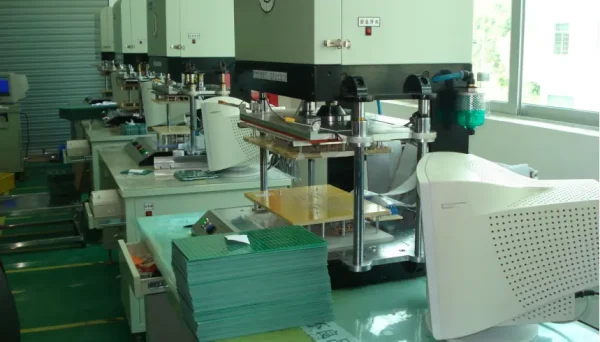
The manufacturer must have the necessary expertise, equipment, and materials to produce the desired type of PCB.
Rigid PCB manufacture, Flexible PCB manufacture and Rigid-Flex PCB Manufacturer are all complex processes that require specialized materials and equipment. Rigid PCB can cover most needs, Flexible PCBs offer more versatility, while rigid-flex PCBs combine the best of both worlds. If you need related services please feel free to contact us, as a well-known brand in the industry, Yingstar is always ready to provide you with the best quality PCB and PCBA products.
Flexible PCB Manufacture Capabilities
FPC Capacity | ||||||||||||||||
Item | Routine | Special | ||||||||||||||
Layers | 1-12 layers | 12 layers above | ||||||||||||||
Board Size(Max) | 500mm×500mm | |||||||||||||||
Board Thickness | 0.060mm—2.5mm | 4mm (Flex-rigid Board) | ||||||||||||||
CNC hole Size(Max) | 6.5mm | |||||||||||||||
CNC Hole Size(Min) | 0.2mm | 0.15mm | ||||||||||||||
CNC Hole Diameter Tolerance | ±0.025mm | |||||||||||||||
CNC Drilling Slot Length and Width Ratio | 2∶1 | |||||||||||||||
Hole(inner) Copper Thickness | Min:10μm | Max:38μm | ||||||||||||||
Min Line Width/ Line Space | 0.075/0.075 mm | 0.05/0.05mm | ||||||||||||||
Etching Tolerance | ±20%( Min Tolerance±0.03mm) | |||||||||||||||
The Accuracy of Graphics to Graphics | ±3mil ( ±0.0762mm) | |||||||||||||||
The Accuracy of Graphics to Holes | ±2mil ( ±0.0508mm) | |||||||||||||||
Cover Film Tolerance | ±8mil (±0.20 mm) | ±4mil(±0.10 mm) | ||||||||||||||
Thermal Curable Ink/UV Ink Location Tolerance | ±0.2mm | ±0.15mm | ||||||||||||||
Green Oil Bridge( Min) | 0.1mm | 0.075mm | ||||||||||||||
Min Electrical Test Pads | 8mil X 8mil | 6mil X 6mil | ||||||||||||||
Outline Dimensions Min Tolerance(Edge-to-Line) | ±0.15mm | ±0.125mm | ||||||||||||||
Finger Edge Spacing | ±0.1mm | ±0.125mm | ||||||||||||||
Outline Dimensions Min Tolerance(Edge-to-Line) | ±0.1mm | ±0.05mm | ||||||||||||||
Min R Angular Radius (Filleted Corner) | 0.2mm | |||||||||||||||


Metal base PCB Manufacture Capabilities
Item | Technical Parameter | ||||||||||||
Material | Aluminum base, copper base, Iron base | ||||||||||||
Surface Finish | Chemical Gold, HASL, Immersion Tin, Chemical Silver, OSP | ||||||||||||
Layer | Single layer, 2 Layer, 4 Layer | ||||||||||||
MAX Size | 1185mm*480mm | ||||||||||||
Min Size | 5mm*5mm | ||||||||||||
Min line space&width | 0.1mm | ||||||||||||
Warpage | ≤0.5%(thickness:1.6mm, size:300mm*300mm | ||||||||||||
Board thickness | 0.3-5.0mm | ||||||||||||
Copper weight | 35um-240um | ||||||||||||
Outline tolerance | ±0.15mm | ||||||||||||
V-CUT tolerance | ±0.1mm | ||||||||||||
Manufacturing capacity | 7000m2/Month | ||||||||||||
Via positioning deviation | ±0.076mm | ||||||||||||
Featured Services
For 2 layer and 4 layer PCB prototypes, we have the shortest lead time and most affordable prices. Our typical lead time for 2 layer samples is 3–4 working days, but in urgent basis, the lead time can be reduced to 24–48 hours depending on your needs. Additionally, our typical lead time for 4 layer samples is 4-5 working days, but in urgent basis, the lead time might be 48 or 72 hours depending on your needs.
Cost-wise, the price can only be within 30-50 USD for two-layer prototypes with maximum dimensions of 100 mm in width, 100 mm in length, and 6 mil line width and space (3-4 working days lead time). Cost can only be 80 USD for 4 layer prototypes with minimum line width & space of 6 mil, width and length no greater than 100mm (4-5 working days). If your PCB is larger than those specifications, we will check the files and give you the best price.
We offer a complete satisfaction guarantee on every job.
Free silkscreen, solder mask, and tooling.No MOQ.
Testing methods
We carry out multiple quality control methods to ensure that the PCBs we are shipping are completely qualified.These testing methods include:
- Visual Inspection
- Flying probe
- Bed of nails
- Impedance control
- Solder-ability detection
- Digital metallographic microscope
- AOI (Automated Optical Inspection)


