
5, Components shifted or misaligned
Inconsistent and mismatched temperatures of the components during the reflow phase can lead to component displacement at the pads.
Common PCB assembly testing methods
- In-Circuit Testing Methods
- Automated Optical Testing
- Boundary scan method
- Built-in self-test
- Aging Test
- X-ray inspection
- PCBA Function testing
- Other PCBA tests
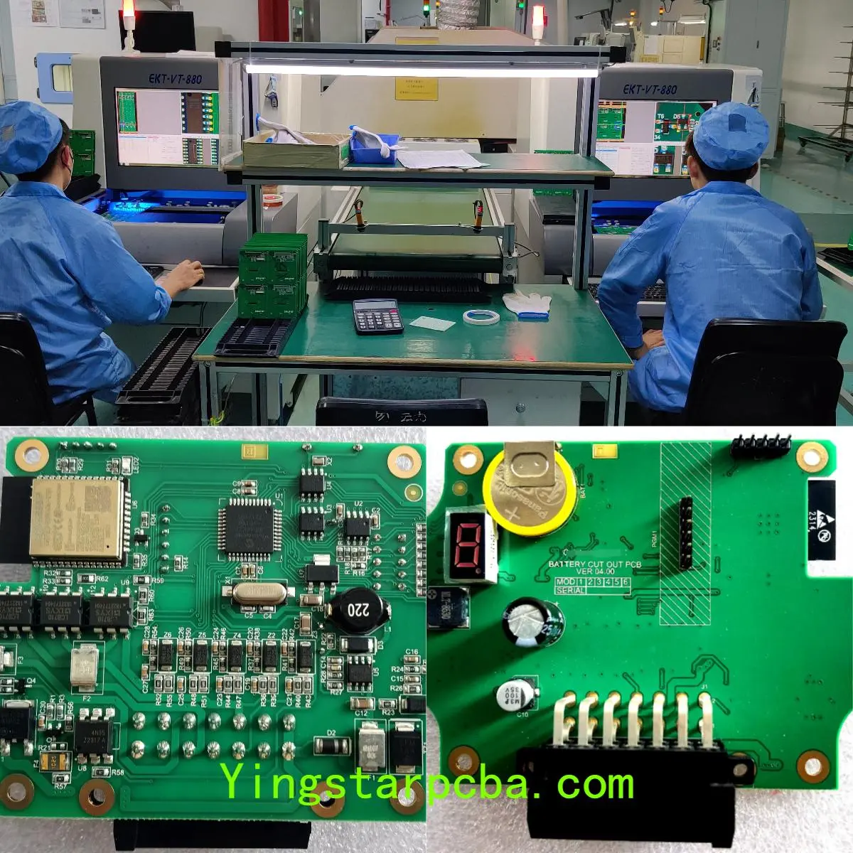
1.Online Test (ICT)
Test time: at the end of PCB assembly
The most common defects that ICT can find include solder shorts, missing components, component failures, lifted leads, displaced components, and poor soldering issues.
Two methods of in-circuit testing – Standard bed of nails testing and Flying probe testing.
Standard bed of nails in-Circuit Test:
Applicable to: PCBs other than modern dense pack boards
Pros: ~85-98% test coverage; can run many parallel test measurements simultaneously
Cons: High machine cost; Difficult to renew nail beds
Flying Probe Test (FICT):
Ideal for: Prototype PCBs, Low to Medium Volume PCBs
Pros: No need for test fixtures for each PCB variant
Cons: longer test cycle time
2. Automatic Optical Inspection (AOI)
Test time: after reflow soldering in SMT assembly
Applicable to: All PCBAs of any volume
Pros: extremely fast and precise
Cons: only tests the surface of the component
Common processes that AOI can detect include missing components, misalignment, misplacement, overall quality, PCB assembly dimensions.
3, Boundary scan method
Stage: After the entire PCB assembly
Applicable to: integrated circuit chip
Pros: Can test JTAG compatible components together
The boundary-scan method, also known as JTAG (IEEE Std 1149.1), is a method for debugging integrated circuit (IC) chips.
4, Built-in self-test (BIST) or built-in test (BIT)
Test time: Final stage of some PCB assemblies
Applicable to: mass production PCB
Pros: high reliability, especially helpful when repairing PCB
Cons: Complicated setup
This is a mechanism that allows the PCB assembly to test itself. Built-in self-test systems not only provide highly reliable testing during production, but also help in later stages, such as when a PCB is being repaired, where these systems can point out problems.
5, Aging test
Test time: After PCB Assembly
Pros: Stimulate the real use of PCBA for a long time
Cons: Takes quite a while depending on demand
This testing method is designed to ensure the reliability and durability of PCBAs under maximum specified stresses and loads. Burn-in testing can detect early failures and can be destructive on the part under test.
6, X-ray inspection (AXI)
Test time: Before and after reflow soldering in SMT assembly
Applicable to: PCBA boards with BGA chips, QFN chips, LGA modules, etc.
Pros: Precise detection of internal defects
Cons: high cost of testing machine
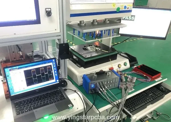
7, PCBA Functional testing
Test time: After PCB assembly
Applicable to: Both bulk PCBAs and prototypes PCBAs
Pros: Covers all behaviors of the end product
The PCBA functional testing bench is composed of test probes, connecting cables, power supply and test software. A functional tester simulates the actual behavior of the PCBA and determines the final pass or fail.
8, Other PCBA tests
Such as IP rating test, drop test, waterproof test, voltage surge test, electromagnetic interference (EMI) test and radio frequency interference (RFI) test, etc., according to the performance of the end product or the use environment.
Is PCBA functional testing necessary for PCBA orders?
If PCBA supplier does not conduct PCBA functional testing before shipment, when you receive your boards, an error suddenly occurs, and your device must be returned to the PCBA supplier to inspect and correct the error. Troubleshooting is a difficult task because AOI testing can only locate surface problems of components and cannot find errors inside PCBAs. So PCBA functional testing is necessary to ensure the highest possible assembly quality.
Why Choose Yingstar to assemble your PCBAs?
Any open connections, defective components, soldering shorts, and any issues on the PCBA can be found and successfully repaired by Yingstar’s senior test engineers during PCBA functional testing.
Yingstar accepts prototypes, small batches, and large batches of PCBA orders and can provide various PCBA test methods according to your needs. If you need a highly professional, good price and quality PCB Assembly supplier, please contact us now.
